CH7511B
- 如果您对产品有相关疑问,或者遇到任何,您都可以注册网站帐号,
- 然后到技术支持论坛去提问寻求帮助。

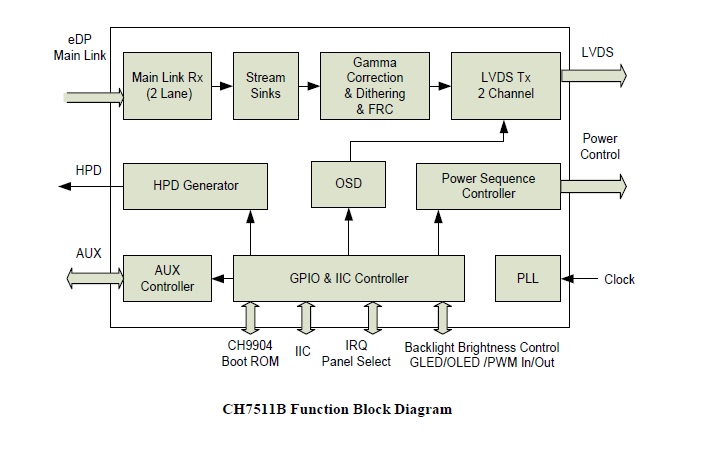
Chrontel’s CH7511B is a low-cost, low-power semiconductor device that translates the Embedded DisplayPort signal to the LVDS (Low-Voltage Differential Signaling). This innovative DisplayPort receiver with an integrated LVDS transmitter is specially designed to target the All-In-One PC and the notebook market segments. Through the CH7511B’s advanced decoding/encoding algorithm, the input eDP high-speed serialized video data can be seamlessly converted to LVDS, a popular display technology for high-speed serial links in mid/large-sized LCD displays. Leveraging the eDP’s unique source/sink “Link Training” routine, the CH7511B is capable of instantly bring up the video display to the LCD when the initialization process is completed between CH7511B and the graphic chip.
The CH7511B is designed to meet the Embedded DisplayPort Specification version 1.2. In the device’s receiver block, which supports two eDP Main Link Lanes input with data rate running at either 1.62Gb/s or 2.7Gb/s, can accept RGB digital formats in either 18-bit 6:6:6 or 24-bit 8:8:8 for LVDS output up to 1920x1200. To comply with GPU’s new power saving scheme such as display frame rate reduction, the CH7511B is equipped with the Dynamic Refresh Rate switching method, which can automatically reduce to the low refresh rate supported by the LVDS panel.
The integrated LVDS transmitter supports the single port and the dual ports LVDS outputs to drive display resolution up to WUXGA (1920x1200). CH7511B supports panel select by GPIO[0:3] pins control or writing the chip registers. To reduce EMI emission, the CH7511B’s LVDS encoder block has incorporated Spread Spectrum control and its spread percentage can be adjusted through the internal registers.
The Backlight On/Off and the PWM are two luminance control functions designed in the CH7511B LVDS power control module. The brightness control commands sent through AUX Channel can be dynamically translated by CH7511B and converted into LCD backlight control signal. The CH7511B will save the last setting of brightness level into the BOOT ROM and restore it upon power up. The CH7511B can dynamically adjust backlight brigntness according to video stream to save power consumption and it supports OSD display in this way.
The CH7511B will immediately convert the eDP signal to LVDS output after eDP Link Training is completed. This feature can be achieved by loading the panel’s EDID and the CH7511B’s configuration settings in the serial BOOT ROM connected to the CH7511B. During system power-up and upon completion of the eDP Link Training through AUX Channel, CH7511B will generate LVDS signal according to the panel power-up timing sequencing stored in the BOOT ROM.
PCB Layout and Design Guide for CH7511B and CH7512B, AN-B014 rev1.7
Commercial and Industrial Grade Products, AN-B037 Rev 1 2
Input Interface eDP/DP
Output Interface LVDS
Audio Interface No
Other features No
Package Type QFN68
Part Number Package Type Operating Temperature Range Minimum Order
CH7511B-BF Lead Free - 68-pin QFNCommercial : 0 to 70°C260 per tray
CH7511B-BFI Lead Free - 68-pin QFNIndustrial : -40 to 85°C260 per tray

传真:86-21-68791558
总公司网站: www.chrontel.com
电子邮件:ke.liu@chrontel.com.cn
微信公众号: 
Copyright © 1998-2023 Chrontel, Inc. All Rights Reserved. 沪ICP备15010045号-1  沪公网安备31011502003526号 隐私保护 法律声明